Ph.D. Research Talks

Mitesh Goyal
(Indian Institute of Science)
Talk Title:
Engineering SCR for better transient characteristics and for high area efficiency
Abstract:
In this talk, various engineering methods to improve the ESD characteristics of SCR are discused. Firstly, a novel gate and substrate triggered silicon-controlled rectifier (SCR) with improved transient characteristics for electrostatic discharge (ESD) protection concepts is presented and secondly, an area efficient implementation of the SCR with tunable trigger voltage is presented. The ESD local protection concepts are presented with co-engineered devices and trigger circuits resulting in lower peak voltages, improved turn-on times and higher area efficiency when compared to known reference ESD protection concepts. Previous works related to SCR have concentrated on quasi static TLP/vf-TLP parts and very little work is published to improve the transient characteristics of the ESD characteristics. The proposed and reference concepts are implemented in Samsung 28 nm process for experimental validation and benchmarking. TLP/vf-TLP and other ESD/DC measurement results along with the design guidelines and trade-offs are presented in this paper. The proposed concept can realize the demanding I/O needs of SCR based local clamps, qualified for HBM to CDM time domains, and meeting ESD specs required for high speed I/Os buffers.

Mayank Yadav
(Indian Institute of Science)
Talk Title:
Junction Engineered FinFET SCR for Ultimate Tunability of Trigger and Holding Voltage
Abstract:
Junction-Engineering for fin-based silicon controlled rectifier (FinSCR) architectures for on-chip ESD protection is proposed in this work to achieve a wide range of holding and trigger voltages without compromising the failure current. In this novel proposal, low dose higher energy deep implants are placed underneath fins. P+ is replaced with an N+ at the Anode/NTAP and N+ with P+ at the Cathode/PTAP of FinSCR to form additional p-n or n-p junctions beneath fins in the n-well and p-well region. These junctions provide the junction potential in the well region to manipulate the bipolar efficiency of parasitic PNP and NPN. Detailed physical insight is explained on holding and trigger voltage tunability for junction-engineere architecture. Besides, the proposed concept, together with the number of fins of the Anode/Cathode or NTAP/PTAP, offers the ultimate tunability.

Harihar Nath
(Indian Institute of Science)
Talk Title:
Physics Based Modeling of Space Charge Modulation Snapback Phenomenon in the TLP Characteristics of HV LDMOS Devices
Abstract:
A physics-based analytical model is developed for capturing the phenomenon of space charge modulation in the intrinsic NPN of the LDMOS device for a 100 ns TLP stress. Reverse-biased base–collector avalanche, current partitioning through the emitter diode and base resistance, and space charge modulation by injected electrons are coupled self-consistently to reproduce the snapback phenomenon and to form the basis for current filament formation. Model Validation was also done by varying the n-well region’s doping.
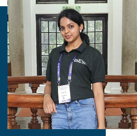
Shravya N Raj
(Indian Institute of Science)
Talk Title:
Why Schottky Contact in LDMOS Protects It From Filament-Driven Catastrophic ESD Failure?
Abstract:
In this work, well-calibrated electrothermal 3D TCAD simulations are used to investigate the behavior of Schottky drain LDMOS devices under ESD stress. The study examines ESD robustness for different Schottky drain metal work functions, with particular emphasis on current filament formation and evolution. The impact of drain-side Schottky barrier engineering is analyzed in detail to identify the appropriate metal silicide for achieving enhanced ESD protection. Transient ESD simulations reveal how variations in barrier height influence carrier injection, current spreading, and localized self-heating, which collectively govern filament stability and failure onset. The results provide physical insight into filament-driven catastrophic failure mechanisms and demonstrate that optimized Schottky drain design can effectively suppress current localization and improve ESD robustness.